
There’s a significant infrastructure upgrade in the works at Amazon, Google, Meta, Microsoft and Nvidia to meet increasing connectivity demands driven by AI/ML. And a significant driver for new AI-era rack redesigns is the energy efficiency, bandwidth improvements and lower latency interconnect improvements now in reach with integrated silicon photonics. But while the performance metric for photonic integrated circuits (PIC) at 800G and 1.6T are well publicized, it’s the need for mass production of laser integration for optical connectivity solutions that is holding back data center transformation.
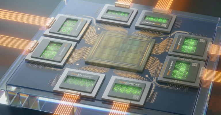
Among the various photonics-based products designed to optimize laser coupling, test schemes and reliability, NewPhotonics NPG102 family of silicon PIC transmitter on chip solutions announced this year is among a select few that feature heterogeneous laser integration. It’s built on a novel laser integration approach that fast tracks a paradigm shift in system design to increase manufacturability of optical PIC products for transceivers. The innovation in NPG102 impacts module production yield maturity and reliability with integrated laser efficiencies and efficacy.
In our novel product implementation of wafer-level heterogeneous laser integration we address transceiver module design issues with new materials that drive elimination of assembly and test steps. With greater than 90% efficiency (<0.5 dB loss) laser coupling, this reduces failure risks and drives scale output of the optical connectivity solutions that data center and hyperscalers are ready to deploy.
Here’s a breakdown of the primary ways our approach will influence quicker adoption of silicon PIC solutions in the data center.
Making the leap to greater coupling gains
There are several techniques for laser coupling including discrete components and integrated technologies. However, discrete laser components require resources and instruments for laser-lens attach, wire-bonder, and auto-aligner that contribute significantly to budgets and production schedules. The problem with most discrete component approaches is that the trade-off in gains also doesn’t deliver the improvements necessary to increase volume manufacturing.
Today’s existing range of coupling methods focuses on discrete components where active alignment and accuracy requirements for external lasers increase the challenges across cost, manufacturability, and scaling for module production.
Moving beyond discrete components is critical, and only possible by intertwining new materials with traditional silicon-based semiconductor technologies. Effective adaptation and adoption of laser integration at the wafer-level is the path to cost, performance, and scalability of solutions with the all-optic connectivity advantage.
Making a material shift in laser integration
We’ve tightened the alignment of laser and waveguide leveraging a novel approach to wafer bonding that integrates the III-V material indium phosphide (InP) onto silicon substrates. This enables laser fabrication directly on silicon photonic platforms. This integration improves precision, density, and manufacturing efficiency.
By optimizing the bonding technique and designing a tailored waveguide form, the transition to III-V lasers and silicon confines light more effectively. Leveraging this SOI substrate innovation with a direct wafer bonding approach that maximizes surface treatment and thermal budgets creates compact and efficient photonic devices with efficient optical coupling and minimized losses.
Match your optical mode
Integrated laser-to-waveguide coupling is a key element in heterogeneous photonic systems. So, the key to effective laser integration that fosters a higher signal quality is optical mode matching.
External lasers in transceivers reach approximately 2.5 dB optical coupling loss due to the mismatch between the non-optimal, asymmetric DFB mode and the symmetric edge coupler input mode. Coupling laser energy output into the waveguide demands an optical mode-matching design that is three-dimensional to optimize optical mode and the power transfer that reduces coupling loss. The alternative in discrete components coupling results in mode mismatch – falling short of the capabilities with laser and waveguide integration.
Addressing barriers driven by mechanical alignment demands accuracy based on time consuming active alignment techniques. Packaging of discrete components in optical transceiver products is slow and labor intensive, resulting in low-volume and expensive technology due in large part to external laser integration.
Advancing laser packaging maturity
Core to our design is help from mature CMOS infrastructure to devise a short cut that eliminates the deficiency in integrated optics technology. Central to the NPG102-design is the InP thin films integrated by way of wafer bonding. Compared with the alignment of a laser diode to a silicon photonic chip in the final stage of packaging, integration of III-V-on-Si lasers represents a major technological breakthrough to produce a practical laser on silicon.
This integration shifts laser functionality from the last manual chip-level production stage to an earlier and automatic CMOS-like manufacturing stage. The profound jump in fabrication precision, integration density, production volume, and efficiency will also enhance laser reliability to become the preferred technology of leading hyperscalers.
Eliminating failure points
Deploying CMOS-like technology with InP laser integration is impactful on device-level and transceiver module reliability and production yield. Laser failure presents the highest potential risk in transceivers, but photonic devices with wafer-level integrated lasers are less susceptible to environmental-triggered failures due to an encapsulated silicon-based process. This paired with the inherent reduction in other discrete components lowers the points of failure at the die-level.
When a new transceiver integration begins with a “Known Good Die” (KGD) the ramp to yield maturity is inherently quicker. When paired with removal of laser coupling and integration resources and skill set demands, this novel integrated laser strategy improves overall production yield metrics, output reliability and consolidated time-to-market. In the highly competitive datacom transceiver market these differentiators are crucial to achieving both efficiency and cost goals.
Take the next leap in laser integration
Wafer-level heterogenous integrated lasers for silicon PIC-based interconnect modules represent a transformative shift in optical transceiver reliability and manufacturability. By leaping beyond discrete component tactics with minimal and discrete gains, we’ve found success addressing critical market growth and sustainability concerns.

With the NPG102 we are making a paradigm shift to bridge the module supply gap for high-capacity, low-latency, and power-efficient data centers in this burgeoning era of artificial intelligence. This evolution is set to redefine data center performance and efficiency, making it an indispensable technology for the future of optical communications and beyond.